Original Link: https://www.anandtech.com/show/11771/intel-announces-movidius-myriad-x-vpu
Intel Announces Movidius Myriad X VPU, Featuring ‘Neural Compute Engine’
by Nate Oh on August 28, 2017 11:00 AM EST- Posted in
- Intel
- SoCs
- Machine Learning
- Movidius
- Neural Networks

Today, Intel subsidiary Movidius is announcing the Movidius Myriad X vision processing unit (VPU), a low-power system-on-chip (SoC) intended for deep learning and AI acceleration in vision-based devices such as drones, smart cameras, and VR/AR headsets. This follows up on last month’s launch of the Myriad 2 powered Movidius Neural Compute Stick. As for the Myriad 2, the Myriad X will coexist alongside its predecessor, which was first announced in 2014. Movidius states that the Myriad X will offer ten times the performance of the Myriad 2 in deep neural network (DNN) inferencing within the same power envelope, while the Myriad 2 will remain a lower performance option.
Under the hood, the Myriad X SoC features what Movidius is calling a Neural Compute Engine, an on-chip DNN accelerator. With it, Movidius states that the Myriad X can achieve over one trillion operations per second (TOPS) of peak DNN inferencing throughput, in the backdrop of the Myriad X’s theoretical 4+ TOPS compute capability.
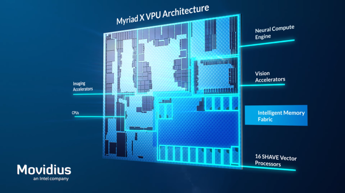
In addition, the Myriad X has four more C-programmable 128-bit VLIW vector processors and configurable MIPI lanes from the Myriad 2, as well as expanded 2.5 MB on-chip memory and more fixed-function imaging/vision accelerators. Like the ones found in the Myriad 2, the Myriad X’s vector units are proprietary SHAVE (Streaming Hybrid Architecture Vector Engine) processors optimized for computer vision workloads. The Myriad X also supports the latest LPDDR4, with the MA2085 variant equipped with only interfaces to external memory. In an accompanying launch video, Movidius locates the Myriad X functions on a stylized dieshot.
Another new function in the Myriad X is 4K hardware encoding, with 4K at 30 Hz (H.264/H.265) and 60 Hz (M/JPEG) supported. Interface-wise, the Myriad X brings USB 3.1 and PCIe 3.0 support, both new to the Myriad VPU family. All this is done within the same <2W power envelope as the Myriad 2, cited more specifically as within 1W.
| Movidius Myriad Family VPUs | ||
| Myriad 2 | Myriad X | |
| Compute Capacity | >1 TOPS | >4 TOPS |
| Vector Processors | 12x SHAVE Processors | 16x SHAVE Processors |
| CPUs | 2x LEON4 cores (RISC; SPARC V8) |
2x LEON4 cores (RISC; SPARC V8) |
| On-chip Accelerators | ~20 image/vision processing accelerators | 20+ image/vision processing accelerators Neural Compute Engine (DNN accelerator) |
| Neural Network Capability | 1st Gen DNN Support (Up to 100 GFLOPS) |
Neural Compute Engine (Up to 1 TOPS) |
| On-chip Memory and Bandwidth | 2 MB (400GB/sec) |
2.5 MB (450GB/sec) |
| DRAM Support | Max: 8Gb LPDDR2 (533MHz, 32-bit) LPDDR3 (933MHz, 32-bit) |
Max: 16Gb LPDDR4 (1600MHz, 32-bit) |
| DRAM Configurations | 1Gbit LPDDR2 (MA215X) 4Gbit LPDDR3 (MA245X) |
No in-package memory (MA2085) 4Gbit LPDDR4 (MA2485) |
| Encoder/Codec | VGA, 720p, 1080p, H.264 (software encoder) | M/JPEG 4K at 60Hz encoder H.264/H.265 4K at 30Hz encoder |
| Key Interfaces | 12x MIPI lanes (DPHY 1.1) USB 3 SPI I2S SD 1GbE |
16x MIPI lanes (PHY 1.2) USB 3.1 Quad SPI I2S 2x SD 10GbE PCIe 3.0 |
| Process | 28nm HPC+/HPC/HPM (TSMC) | 16nm FFC (TSMC) |
| Package | 6.5mm x 6.5 mm (MA215X) 8mm x 9.5 mm (MA245X) |
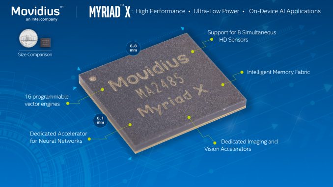
8.1mm x 8.8mm (MA2085, MA2485) |
At a glance, much of the Myriad X’s extra performance at the same Myriad 2 power appears to come from its new 16nm FFC TSMC process node. In shrinking from a 28nm planar process to 16nm FinFET, Movidius was able to invest the power savings into higher performance as well as more SHAVE processors, accelerators, interfaces, and memory, all in a relatively similar package size. While Intel indeed has its own fabs, Movidius stated that the Myriad X was in development well before Intel acquired Movidius in 2016, and thus 16nm FFC was the technology of choice. This 16nm FFC iteration comes after the Myriad 2’s incarnations on three of TSMC's 28nm process variants: HPM, HPC, and HPC+.
While specifics were not disclosed, the Myriad X VPU comes with an SDK that includes a neural network compiler and “a specialized FLIC framework with a plug-in approach to developing application pipelines.” In any case, like the Myriad 2, the Myriad X will be programmable via the Myriad Development Kit (MDK). At this time, there were no details about the reference kit hardware.
As mentioned earlier, the Myriad 2 will not be replaced by the Myriad X. Last January, the Myriad 2 was described as costing under $10; based on the higher cost FinFET process and additional hardware features, the Myriad X will likely command a higher price for the higher performance.
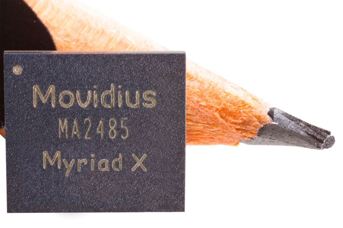
Update (8/28/17): An Intel representative has given an update stating that 8.1mm x 8.8mm are the correct dimensions for the Myriad X VPUs. The original specifications (8.5mm x 8.7mm) that were given out were incorrect. The press kit photo has been updated.
Source: Movidius


